Range of application
One of the core competencies of JEOL, which it has been developing and manufacturing for several decades, is transmission electron microscopes (TEM). This long tradition has created the expertise required to be able to offer world market leading products in this field. Many years of close global collaboration with research institutes and industry has resulted in extremely stable TEMs, which provide the highest resolution. JEOL TEMs can be used for a wide range of applications, be that developing cutting-edge materials or determining the structure of life's building blocks.
Solutions
- Suitable for all samples capable of radiography treatment
- Atomic resolution of materials
- Examination of biological samples at room and low temperatures
- In-situ examinations and characterisation of new material groups
- Classification of molecule structures for developing new medicines


Detailed solutions
- 3D reconstruction of biological micro- and nanostructures
3D reconstruction of biological micro- and nanostructures
The resolution of conventional optical microscopes and x-ray tomography systems is insufficient to understand the structural information of biological samples on a micro- and nanoscale. With JEOL electron microscopes it is possible to image and three-dimensionally reconstruct not only the smallest of biological structures such as viruses, but also microscale objects such as synapses or cells.
Product groups
Transmission Electron Microscopes (TEM)
Solutions
 Reconstruction of a bacteriophage (left) and synapses (right)
Reconstruction of a bacteriophage (left) and synapses (right)
Source data: Journal of Structural Biology 177 (2012) 589–601 and JEOL News 51
- Analysing nanoparticles #2
Analysing nanoparticles #2
Due to their unique properties, nanoparticles are becoming increasingly important in industry as well as university research. Their chemical and physical properties depend heavily on their size, shape and composition. With the high-performance instruments from JEOL, these properties can be reliably analysed, even down to the sub-nanometer range.
Product groups
Transmission Electron Microscopes (TEM)
Solutions
 Electron microscope image of an iron oxide nanoparticle
Electron microscope image of an iron oxide nanoparticle
Source data: JEOL (Germany) GmbH, Bielefeld University, Dr. Ennen / Applied Research Paper F200
- Analysing nanoparticles
Analysing nanoparticles
Due to their unique properties, nanoparticles are becoming increasingly important in industry as well as university research. Their chemical and physical properties depend heavily on their size, shape and composition. With the high-performance instruments from JEOL, these properties can be reliably analysed, even down to the sub-nanometer range.
Product groups
Transmission Electron Microscopes (TEM)
Solutions
 Element core-shell nanoparticle. The inner gold core (red) is covered by a 0.6 mm thin palladium layer (green).
Element core-shell nanoparticle. The inner gold core (red) is covered by a 0.6 mm thin palladium layer (green).
Source data: JEOL Ltd. / GrandARM presentation
- Asbestos analysis
Asbestos analysis
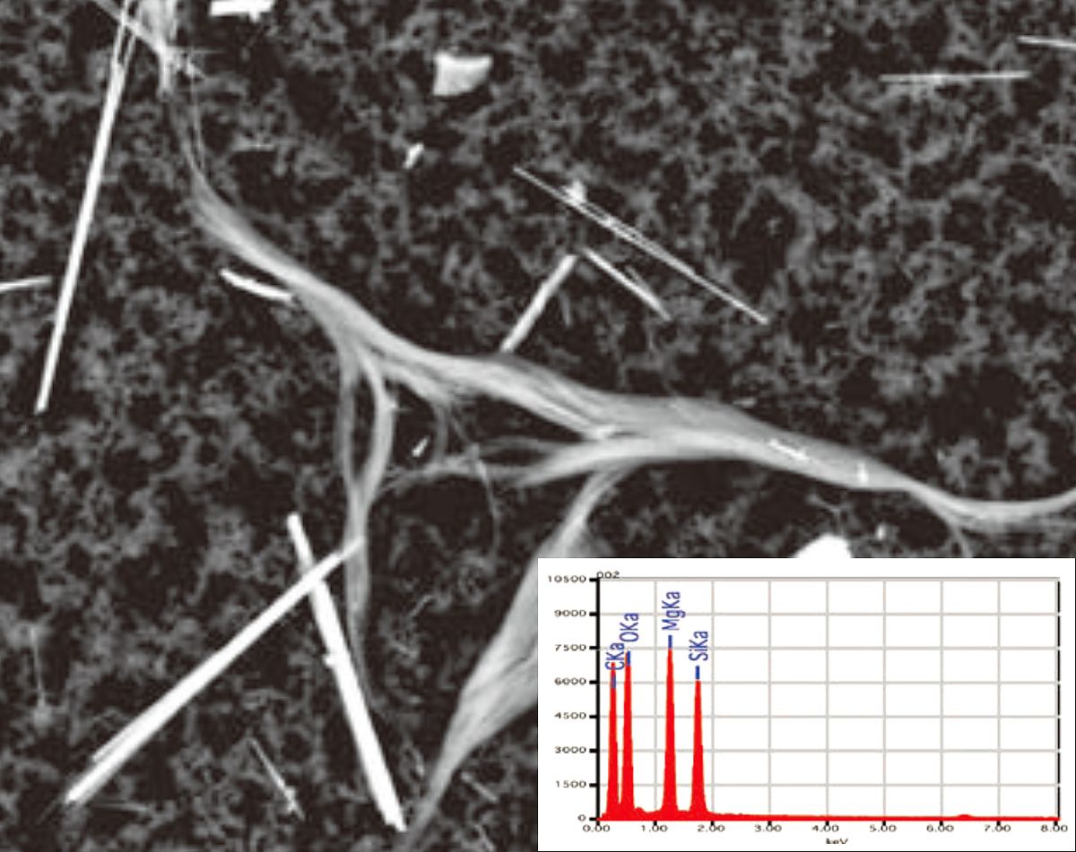
Asbestos was used for decades as a fire- and temperature-proof raw and insulation material. Once the health risks were discovered, many laboratories examined potentially asbestos-containing construction materials. JEOL is the only manufacturer to offer the powerful combination of its own electron microscopes and own spectrometers as a complete solution for standards-compliant asbestos analysis.
Product groups
Transmission Electron Microscopes (TEM)
Solutions
 Identification of a chrysotile fibre by means of SEM imaging and EDX spectrum
Identification of a chrysotile fibre by means of SEM imaging and EDX spectrum
Bildquelle: JED-Broschüre
- Characterising biomolecules #2
Characterising biomolecules #2
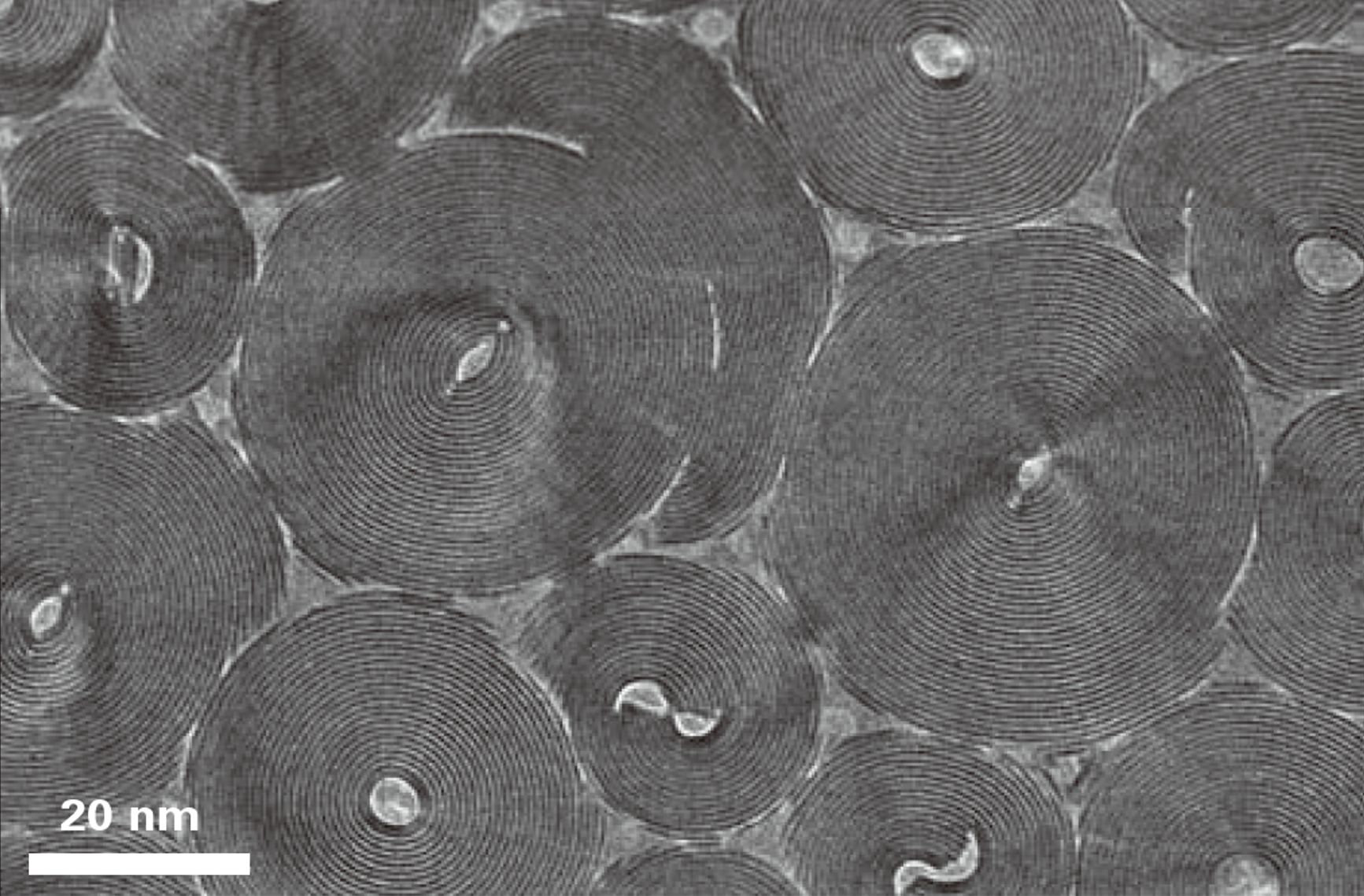
Cryo electron microscopy and the analysis of protein structures has undergone drastic changes since the last years. This technique was awarded the Nobel Prize in Chemistry 2017 (https://www.nobelprize.org/nobel_prizes/chemistry/laureates/2017/advanced-chemistryprize2017.pdf).
With the introduction of fast and highly sensitive camera techniques as well as dedicated, automated electron microscopes resolutions of 2 Ångström and lower could be achieved under near to native conditions. This single particle analysis method (SPA) allows to efficiently determine the structure of non crystalline proteins in order to design new drugs or to resolve the fundamental functions of biochemical or molecular biological processes.Product groups
Transmission Electron Microscopes (TEM)
Solutions
 GroEL protein at 40k x magnification (pixel size 0.12 nm), detector: K2 summit, instrument: CRYO ARMTM200, Schottky 200kV, inset: reduced live FFT, zero-loss image with 20eV slit width
GroEL protein at 40k x magnification (pixel size 0.12 nm), detector: K2 summit, instrument: CRYO ARMTM200, Schottky 200kV, inset: reduced live FFT, zero-loss image with 20eV slit width
Source data: JEOL Ltd., University Osaka, Prof. Namba
- Characterising biomolecules
Characterising biomolecules
DNA origami is a new technology in synthetic biology, or rather the disciplines of biochemistry and biophysics. It involves DNA molecules being turned into random two- and three-dimensional nanoforms. These synthetically folded DNA molecules are used as e.g. future biocompatible carriers for active substances or to produce nanomachines or nanorobots.
Product groups
Transmission Electron Microscopes (TEM)
Solutions
 Negatively contrasted TEM image of synthesised DNA molecules
Negatively contrasted TEM image of synthesised DNA molecules
Source data: JEOL (Germany) GmbH, Technical University of Munich, Prof. Dietz and Klaus Wagenbauer.
- Characterising precipitates
Characterising precipitates
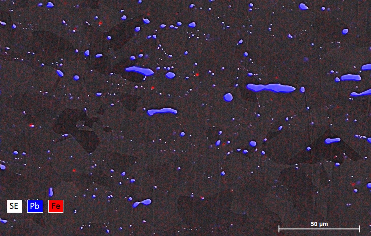
The formation of precipitates is used systematically to define the mechanical properties of a metallic structure. However, as a form of contamination, these can also be undesired. In order to be able to judge the quality of an alloy, it is necessary to determine the morphology and chemical composition of the precipitates. This is why JEOL supplies all-round, complete solutions, from artifact-free sample preparation to high-resolution analysis from the µm to the nm level.
Product groups
Transmission Electron Microscopes (TEM)
Solutions
 Element mapping image of a brass alloy
Element mapping image of a brass alloy
Source data: JEOL (Germany) GmbH
- Element analysis
Element analysis
Magnetotactic bacteria orientate themselves along the Earth's magnetic field with the help of magnetite particles enveloped in a membrane. These organisms serve as a model for examining the complex processes of biomineralisation. Entities known as magnetosomes (comprising magnetite crystal and membrane) are also tested as carriers for active substances and for new forms of therapy in medicine (hyperthermia therapy). JEOL supplies combined and fully automated solutions for the high-resolution elementary classification of the individual constituents.
Product groups
Transmission Electron Microscopes (TEM)
Solutions
 Element analysis (red rectangle) at 120 kV in S(TEM) on magnetotactic bacteria, magnetite chains (green)
Element analysis (red rectangle) at 120 kV in S(TEM) on magnetotactic bacteria, magnetite chains (green)
Source data: JEOL (Germany) GmbH
- Fibre analysis
Fibre analysis
Fibres are used in many branches of industry, e.g. in textile processing or as a structural material in mechanical engineering. Their structural properties can be studied by means of a fibre cross-section, for example. JEOL supplies an established and powerful complete solution for simple, artifact-free preparation and high-resolution imaging and analytics.
Product groups
Transmission Electron Microscopes (TEM)
Solutions
 SEM image of a cross-section through a fibre bundle
SEM image of a cross-section through a fibre bundle
Source data: JEOL Ltd., Ion Slicer brochure
- Graphene analysis
Graphene analysis
The atomic imaging and analysis of light, electron-beam-sensitive materials requires high-performance microscopes. Thanks to their high stability and outstanding resolution, JEOL transmission electron microscopes are even capable of effortlessly identifying and examining lattice defects between individual carbon atoms.
Product groups
Transmission Electron Microscopes (TEM)
Solutions
 Atomic resolution image of graphene
Atomic resolution image of graphene
Source data: JEOL Ltd., GrandARM presentation
- High-resolution 3D reconstruction
High-resolution 3D reconstruction
High-resolution 3D images are essential for understanding the complex interrelationships of biological samples. With JEOL transmission electron microscopes it is possible to image sensitive biological structures without damaging them and reconstruct them by fully automated means in all three spatial dimensions. The calculated 3D model can be virtually moved, segmented and examined in any direction for a simple interpretation.
Product groups
Transmission Electron Microscopes (TEM)
Solutions
 Electron microscope image and reconstructed model of a Golgi apparatus of a threadworm
Electron microscope image and reconstructed model of a Golgi apparatus of a threadworm
Source: JEOL (Germany) GmbH, ENI / Göttingen
- High-resolution bonding state analysis
High-resolution bonding state analysis
The properties of materials are essentially determined by their structure and the bonding states of the atoms. Precise knowledge of the structure and chemical composition are of key importance for the development of new materials. With the high-resolution spectroscopy systems from JEOL, it is possible to examine such bonding states locally with atomic precision.
Product groups
Transmission Electron Microscopes (TEM)
Solutions
 Energy loss spectrum of the minerals rutile (red) and anastase (grey)
Energy loss spectrum of the minerals rutile (red) and anastase (grey)
Source data: JEOL Ltd., ARM200F presentation
- Light element analysis
Light element analysis
The combination of JEOL-patented TEM and EDX systems enables the detection of elements into the nm and sub-nm range. Modern techniques make it possible to achieve an accurate statement about the chemical composition within a very short time. This allows a time-efficient response to problems and questions.
Product groups
Transmission Electron Microscopes (TEM)
Solutions
 Chemical element mapping of a semiconductor sample (JEM-2800)
Chemical element mapping of a semiconductor sample (JEM-2800)
Source data: JEOL (Germany) GmbH, Demoreport AMS AG
- Pinpointing fluorescently labelled proteins
Pinpointing fluorescently labelled proteins
The linking of light microscopy signals and electron-optical details allows, among other things, conclusions to be drawn regarding the exact location of proteins in specific sections of tissues. JEOL manufactures intuitive, multi-system complete solutions for combining fluorescence and high-resolution electron microscopy.
Product groups
Transmission Electron Microscopes (TEM)
Solutions
 Thin section of a zebra fish: correlatively superimposed electron and fluorescence microscopic images
Thin section of a zebra fish: correlatively superimposed electron and fluorescence microscopic images
Source data: JEOL (Germany) GmbH, Centre for Regenerative Therapies, TU Dresden.
- Semiconductor analysis
Semiconductor analysis
In modern semiconductor components, complex, functional structures have to be installed in an ever smaller space. In order to be able to reliably pinpoint and identify faults, it is essential to analyse precisely the structure and the element map. With the automated systems from JEOL, it is possible to prepare, image and analyse semiconductor components for faults precisely with the greatest accuracy.
Product groups
Transmission Electron Microscopes (TEM)
Solutions
 Three-dimensional element map of a NAND circuit
Three-dimensional element map of a NAND circuit
Source data: JEOL Ltd., JEM-2800 brochure/presentation
- Tissue diagnostics
Tissue diagnostics
As part of a biopsy, tissue is removed and subsequently examined under the microscope. Labels can also be used to pinpoint the location of active substances to be examined. JEOL not only supplies specially developed, automated systems for simple and high-constrast imaging and high-resolution and ultrastructural diagnostics. With highly sensitive JEOL EDX detectors, it is also possible to pinpoint the location of the labels used.
Product groups
Transmission Electron Microscopes (TEM)
Solutions
 TEM image of a tissue section
TEM image of a tissue section
Source: JEOL (Germany) GmbH, Demo Friedrich Baur Institut in Munich
- Writing and characterising semiconductor systems
Writing and characterising semiconductor systems
Photolithography is an essential method in semiconductor and microelectrical technology for manufacturing integrated circuits with high throughput. Electron-optical systems from JEOL enable fast, reliable quality assurance, as well as the optimisation and development of new processes in semiconductor technology.
Product groups
Transmission Electron Microscopes (TEM)
Solutions
 Photolithographically structured silicon wafer
Photolithographically structured silicon wafer
Source: JEOL (Germany) GmbH, Max-Planck-Institut für Halbleiterforschung, Munich.
